Scanning Probe Microscopy
Scanning Probe Microscopy and film growth
The SPM group is a part of Axis 1: « Elaboration of innovative materials and new characterization methods ».The SPM group explores the possibility of constructing functioning electronic devices with dimensions on the nanometer scale by using both Scanning Probe Microscopy (SPM) and Pulsed Laser Deposition system (PLD). This multi-disciplinary field brings together fundamental and applied research, physics, chemistry and engineering. The core of the SPM group consists of scanning probe microscopes (in air or under high vacuum) to study new materials based on thin films, superlattices, and nanostructures obtained by PLD and electronic or optical littography.
Thin films are used extensively in electronic device technologies. Understanding the physics of thin film deposition process is therefore critical to much of modern microelectronics technology. Using Scanning Probe Microscopy (SPM), we will gain some insight into the basic mechanisms of film growth. This technique is capable of very high spatial resolution down to the atomic scale under some conditions.
In addition, the laboratory is equipped with a transfert chamber which provides to directly bring the sample from the PLD system into the UHV microscope.
Microscopes
The laboratory is equipped with two microscopes:
- NT-MDT AFM (SMENA in air ):
- Omicron AFM-STM (VT-Beam deflexion) with Spechs electronics:

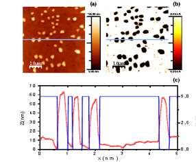
(a) Contact SFM topography image of a LaSrMnO thin film grown on a STO substrate at 1000°C during 12h with the nonmagnetic-insulating (LaSr)0 nanodots imaged on the surface. (b) Contact SFM image corresponding to the same surface displayed in a) at VTip = +2.7 V. (c) Profile following the line indicated in (a) and (b) of the topography and the current measured with Contact SFM. The maximum current is limited to Imax = 5 nA by the current amplifier.

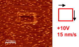
Contact SPM topography image at T = 120 K after the writing process (Voltage V = 10 V). Writing process (voltage applied between the tip and the sample V = 10V).

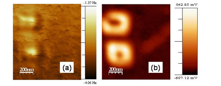
Non Contact MFM image (a) and KPM image (b) on the same surface. Note : Separation between electrostatic and magnetic forces was not evidenced.
Contact
Antoine RUYTER
antoine.ruyter@univ-tours.fr
Laboratoire GREMAN UMR CNRS 7347
Pôle EMA
Université de Tours
Parc de Grandmont
37200 TOURS
FRANCE
Phone : +33 (0) 247 366 939
Mobile : +33 (0) 673 782 640
Fax : +33 (0) 247 367 121
antoine.ruyter@univ-tours.fr
Laboratoire GREMAN UMR CNRS 7347
Pôle EMA
Université de Tours
Parc de Grandmont
37200 TOURS
FRANCE
Phone : +33 (0) 247 366 939
Mobile : +33 (0) 673 782 640
Fax : +33 (0) 247 367 121
