Wide bandgap materials and devices
Wide bandgap materials are ideal candidates for power applications, due to their properties such as: high saturation velocity, high critical electric field…
Research on wide bandgap materials in GREMAN has been initiated in 2004. Since the beginning of the activity, our team is working on process and characterization development on silicon carbide (SiC), gallium nitride (GaN) and zinc oxide (ZnO).
Research on wide bandgap materials in GREMAN has been initiated in 2004. Since the beginning of the activity, our team is working on process and characterization development on silicon carbide (SiC), gallium nitride (GaN) and zinc oxide (ZnO).
Silicon carbide (SiC)
Silicon carbide (SiC) is avowed as an interesting material for high-power and high-temperature applications because of its significant properties including its wide bandgap energy and high temperature stability. SiC is also professed as an ideal candidate for microsystem applications due to its excellent mechanical properties and chemical inertia, making it suitable for harsh environments.
Electrical applications
Due to its excellent electrical, mechanical and chemical properties, silicon carbide coulb ne integrated into electronic devices. For this thematic, a 4H-SiC Junction Barrier Schottky (JBS) diode has been preferred as a vehicle test. The development of such an electronic component requires to control technological issues like doping, ohmic contacts, Schottky contacts, passivation...
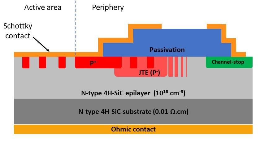
1. Schematic of a SiC JBS diode achieved thanks to the CERTeM platform.
To improve the electrical characteristics, some technological issues are still under investigation. For example, in the frame of the European project WInSiC4AP, we are working on the backside ohmic contact by means of a laser irradiation. Thanks to this method, it is possible to obtain an ohmic contact on thinned SiC wafers, leading to improved electrical characteristics through the reduction of the SiC substrate resistive contribution.
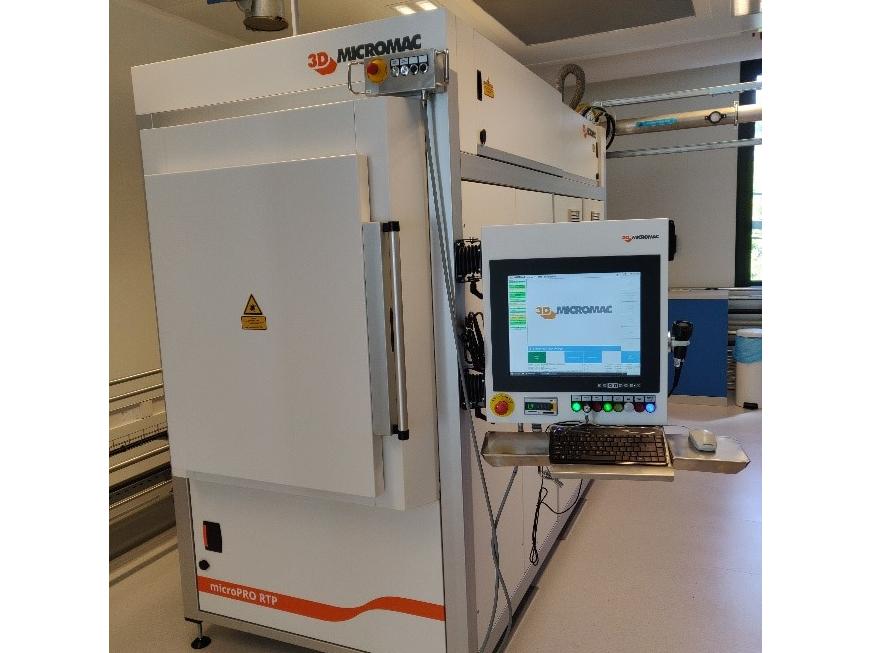
2. Laser tool dedicated to the achievement of ohmic contacts on silicon carbide wafers.
Our team has also developed an expertise for the characterization of doping in semi-conductor materials at the nanoscale, with the electrical modes based on Atomic Force Microscopy (AFM). For example, this expertise has led to the demonstration of the electrical activity of extended defects in 3C‑SiC, thanks to the Scanning Spreading Resistance Microscopy (SSRM) method.
c.
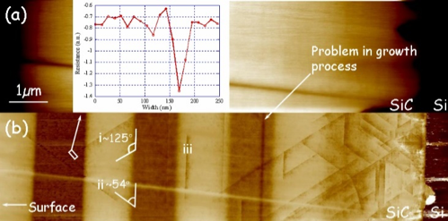
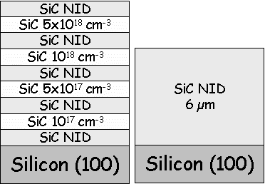
3. AFM topography (a) and corresponding SSRM cartography (b) of a 3C-SiC sample with the nitrogen doping sequence presented in (c). This result clearly highlights that the electrical activity of the extended defects in 3C-SiC can be estimated to be much higher than the one of 5x1018 cm-3 n-type doped layer (from X. Song et al., Applied Physics Letters 96, 142104, 2010).

1. Schematic of a SiC JBS diode achieved thanks to the CERTeM platform.
To improve the electrical characteristics, some technological issues are still under investigation. For example, in the frame of the European project WInSiC4AP, we are working on the backside ohmic contact by means of a laser irradiation. Thanks to this method, it is possible to obtain an ohmic contact on thinned SiC wafers, leading to improved electrical characteristics through the reduction of the SiC substrate resistive contribution.

2. Laser tool dedicated to the achievement of ohmic contacts on silicon carbide wafers.
Our team has also developed an expertise for the characterization of doping in semi-conductor materials at the nanoscale, with the electrical modes based on Atomic Force Microscopy (AFM). For example, this expertise has led to the demonstration of the electrical activity of extended defects in 3C‑SiC, thanks to the Scanning Spreading Resistance Microscopy (SSRM) method.
c.


3. AFM topography (a) and corresponding SSRM cartography (b) of a 3C-SiC sample with the nitrogen doping sequence presented in (c). This result clearly highlights that the electrical activity of the extended defects in 3C-SiC can be estimated to be much higher than the one of 5x1018 cm-3 n-type doped layer (from X. Song et al., Applied Physics Letters 96, 142104, 2010).
MEMS devices
Due to its unique mechanical and physical properties, silicon carbide is also an ideal candidate to achieve Micro-Electro-Mechanical-Systems (MEMS).
More details on the project available here.
Zinc oxide (ZnO)
Electrical applications
Studied at GREMAN for the mechanical energy harvesting application, zinc oxide (ZnO) nanowires (NWs) obtained by hydrothermal synthesis (HS) method were also characterized electrically via single-NW Field Effect Transistors (NW-FET).For the extraction of electrical properties of NWs, we have fabricated bottom-gate single ZnO NW-FET on highly doped Si substrates with 170 nm thick thermally grown SiO2. Fabrication of ZnO NW-FET devices is done using standard electron-beam lithography (EBL) process (3).
Using the IDS-VGS transfer characteristics, important electrical data of the semiconductor NWs, such as mobility and charge density can be extracted1.
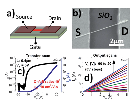
1. (a) Schematic illustration of the single ZnO NW-FET structure. (b) SEM image of a representative single ZnO NW device. (c) Transfer scan in both semi-log (left) and lin–lin scale (right). (d) Family of output scans at VG = -60 to 20V (5V steps) for the same device1.
A key issue of the low temperature HS is that such NWs typically show unacceptable levels of defects (optical and electronic), rendering them inferior to their high temperature counterparts (e.g. vapour-liquid-solid or vapour-phase epitaxy synthesized NWs). Whilst there appears to be no general consensus, it is generally accepted that Zn interstitials, oxygen vacancies and unintentional contamination (H and hydroxyl species) are chiefly responsible for the defects in the crystal. One solution to mitigate the limitations of hydrothermal ZnO NWs is to perform post annealing in oxygen rich ambient. In 1 we demonstrated high performance FETs and practical ohmic and Schottky contacts based on hydrothermal ZnO NWs, where the high carrier concentration was greatly suppressed by a simple low cost thermal annealing step in ambient air at 450°C. Single ZnO NW FETs with Al as source and drain (S/D) incorporating these modified NWs were characterized, showing excellent performance metrics, including low off-state currents (pA range), high on-state current (10 µA at 5 V drain bias), steep subthreshold swing (600 mV per dec), good field-effect carrier mobility (10 cm2V-1s-1) and an effective carrier concentration of 3.7 x 1017cm-3.
Nevertheless, a multiple step manufacturing process was developed where ZnO nanosheets (NS), synthesized by Vapor-Liquid-Solid (VLS) on r-plane Sapphire substrates, were incorporated to flexible FETs with high performance and operational stability2. The VLS synthesized ZnO NSs were drop-casted on both rigid (Si/SiO2) and flexible (PET) substrates, before final steps to obtain back-gate rigid NS-FETs and top-gate flexible NS-FETs respectively. For the latter, parylene C (170 nm thick) was used as top-gate dielectric material. Such devices are found to consistently show very high on-state currents (Ion) > 40 μA, high field-effect mobility (μeff) > 200 cm2V-1s-1, exceptionally high on/off current modulation ratio of around 109, steep subthreshold swing (s-s) < 200 mV/decade, very low hysteresis, and negligible threshold voltage shifts with prolonged electrical stressing (up to 340 min).
More recently, a new type of transistors operation has been introduced by Shannon and Gerstner, called “source-gated transistor (SGT)”. The SGT exploits the reverse bias Schottky diode, present at the source contact, to achieve very early drain current saturation and high internal gain. We demonstrated3 the assembly of SGTs based on single-crystalline ZnO sheets (length between 5 and 25 µm) with asymmetric ohmic drain and Schottky source contacts (2). Electrical transport studies of the fabricated devices show excellent field-effect transport behaviour with abrupt drain current saturation at low drain voltages well below 2 V, even at very large gate voltages.
All these studies deliver concepts for integrating high-quality ZnO nanostructures as active semiconducting elements in flexible electronic circuits.
![Schematic/AFM image, cross-sectional device structure and experimental characteristics of a SGT [Dah16]](https://greman.univ-tours.fr/medias/photo/graphe_1599057613943-png?ID_FICHE=341662)
![Schematic/AFM image, cross-sectional device structure and experimental characteristics of a SGT [Dah16]](https://greman.univ-tours.fr/medias/photo/graphe-2_1599058006552-jpg?ID_FICHE=341662)
![Schematic/AFM image, cross-sectional device structure and experimental characteristics of a SGT [Dah16]](https://greman.univ-tours.fr/medias/photo/graphe-3_1599058057327-png?ID_FICHE=341662)
![[style3;Devices]Since the beginning of the activity in 2004, our team is working on process and characterization development with a clear positioning: Wide Band Gap materials and devices at a low cost.](https://greman.univ-tours.fr/medias/photo/graphe-4_1599058256810-jpg?ID_FICHE=341662)
2. Schematic/AFM image, cross-sectional device structure and experimental characteristics of a SGT.
NEMS devices
ZnO NWs grown using low temperature hydrothermal synthesis were also integrated into nanogenerators, for mechanical energy harvesting purpose. This project is part of the Operation of Research MEMS/NEMS, from design to characterization.Gallium Nitride (GaN)
Gallium Nitride (GaN) is an attractive semiconductor. Recently, electronic devices based on GaN technology for high power and high temperature functioning have been investigated. Due to its wide energy gap and high electron-saturated drift velocity, superior than Si properties, GaN based devices are good candidates for power devices with higher performances in terms of current density or reverse breakdown voltage for example.
ECOSYM team works on the implantation in GaN (to obtain an insulating or semi-insulating layer, activate dopants, mainly P-type), the creation of Ohmic and Schottky contacts, and the optimization of the passivation process for the lateral structure. The team manufactures and characterizes the lateral diodes in the CERTeM clean room.
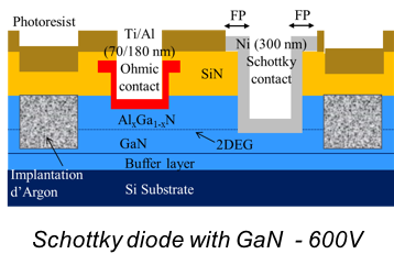
First lateral diodes AlGaN/GaN 600V obtained on a 6 and 8" substrate.
ECOSYM team works on the implantation in GaN (to obtain an insulating or semi-insulating layer, activate dopants, mainly P-type), the creation of Ohmic and Schottky contacts, and the optimization of the passivation process for the lateral structure. The team manufactures and characterizes the lateral diodes in the CERTeM clean room.

First lateral diodes AlGaN/GaN 600V obtained on a 6 and 8" substrate.
