
Synthesis and applications of porous semi-conductors
Example of applications
1) Porous nanoparticles synthesis
The highest specific surface area ever measured for porous silicon (1125 m²/g) was reached using new HF electrolyte compositions [A. Loni et al., in J. of Solid State Science & Technology, Vol. 4, No 8, pp. P289-P292, 2015]. These particles are highly photoluminescent [J. Joo et al. , in Applied Physics Letters, Vol. 108, 153111, 2016]. This work was performed in collaboration with Prof. Leigh Canham (Birmingham, UK) and Prof. Michael Sailor (San Diego, USA).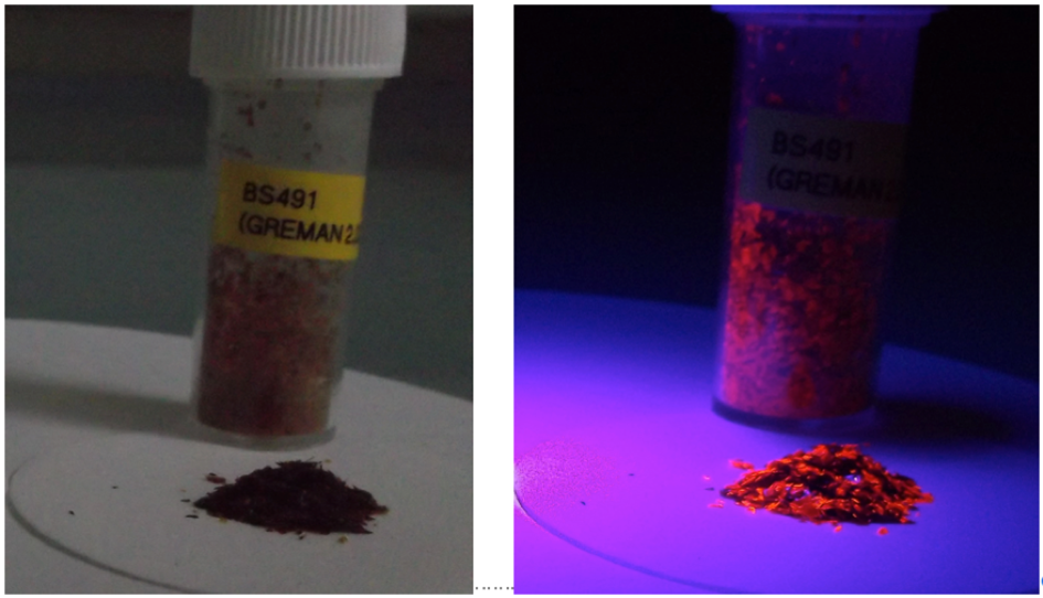
Photoluminescence of PS particles under UV light.
2) Radio-frequency device fabrication
The first realization of a hybrid porous silicon/silicon substrate for RF applications was achieved [M. Capelle et al., in Appl. Phys. Lett. 104 pp. 072104-1-4, 2014]. This work was done in collaboration with STMicroelectronics Tours on 6 and 8 inches silicon wafers. These substrates lead to significant performance enhancement.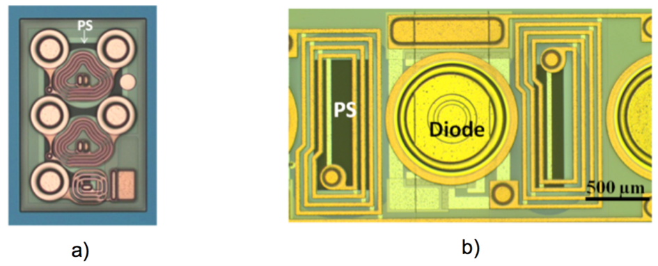
RF circuits prototypes integrated on silicon / PS hybrid substrates. a) Common mode filter and ESD protection diode. b) Low pass filter and ESD protection diode. Components commercialized by STMicroelectronics.
3) Porous Insultation Grids for power electronics
Porous Insulation Grids for power electronics are realized starting from P++ wells fabricated by TGZM (Temperature Gradient Zone Melting), which become the perfect material for the realization of mesoporous Si [G. Gautier et al., in App. Phys. Lett. 88, 212501, 2006]. The P++ wells formed by the thermomigration of Aluminium through silicon wafers are localized and constitute the perfect track for Si etching. Porous Si forms with extremely high conformity by the defined P++ lines.
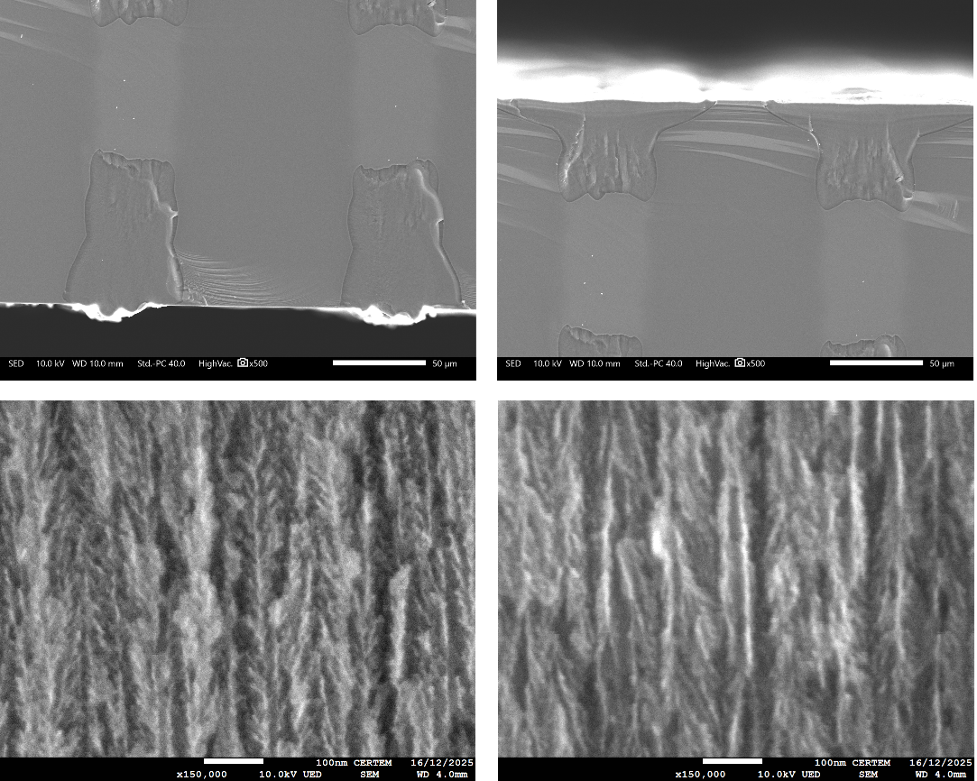
Sideview of porous Si wells made out of electrochemical etching of P++ TGZM grids. Focus on both the entrance (above) and exit (below) sides at low and high magnification.
The Process Implementation in 6-inch Technology is a specificity of the GREMAN. Porous Si fabrication is achievable in a few tens of minutes, reaching etching rates of 10-15 µm/min. The porous Si structures are realized on both sides of a 6-inch wafer in one single run, thanks to the double tank cell geometry designed by AMMT® and the GREMAN. Moreover, the porous Si layers realized all across the wafer enhances the mechanical resistance by reducing the curvature that occurs during the high temperature thermal treatment due to the TGZM process. The experiments are still ongoing within the project IPCEI ME-CT SiGaN4power, making advancements in the implementation of the whole process employing a full device 6-inch wafer.
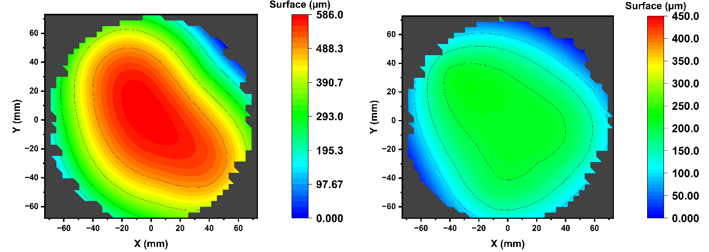
Metrology 6-inch wafer height distribution before (left) and after (right) porous Si grids fabrication.
4) Ultrasonic transducers
The potential of PS film integration on the rear side of ultrasonic transducers to enhance the device performances has also been investigated. Micro-pyramids were etched into silicon wafers, followed by porous silicon layer formation using electrochemical or metal-assisted chemical etching. The optimized structure achieved 26 dB attenuation at 25 MHz, enabling compact transducers with a 26 MHz center frequency and 86% fractional bandwidth. B-mode imaging of an 80 µm tungsten wire confirmed no additional echoes, validating its potential for high-frequency medical imaging. [Defforge et al in J. Micromech. Microeng. Vol. 36, pp. 055008, 2026]
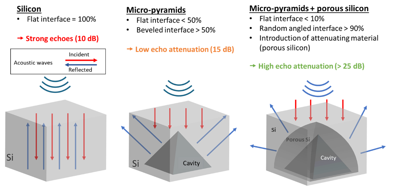
Scheme representing the influence of silicon surface multiscale structuration for the attenuation of echoes imputed to acoustic wave reflections in the substrate.
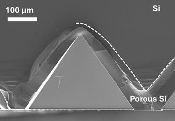
SEM cross-sectional view of multiscale structured silicon substrate, comprising the formation of micro-pyramids and porous silicon layer on the sidewalls of the pyramids to enhance the attenuation of acoustic wave in silicon substrates.
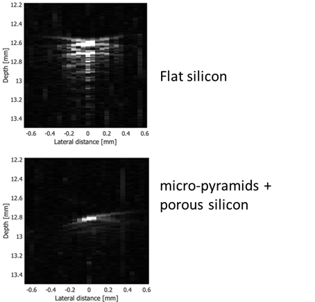
Acoustic images of a tungsten wire. On flat silicon, the echoes cause unwanted diagonal stripes on the image while attenuation these echoes using multi-scale structured silicon significantly reduces the formation of these stripes.
5) Pore coating by atomic layer deposition
We develop atomic layer deposition (ALD) strategies to functionalize porous silicon with ultrathin conformal coatings. These coatings can provide specific properties such as surface passivation, chemical stability, electrical insulation, catalytic activity or charge transport control, depending on the targeted application.
Recent work in the group has focused on the deposition of ultrathin TiO₂ layers on macroporous silicon films. This approach is being investigated for photocatalysis and photoelectrochemical applications, including porous photoanodes for artificial photosynthesis [Al Chimali et al. Mater. Adv., vol. 5, pp. 9270-9278 2024]
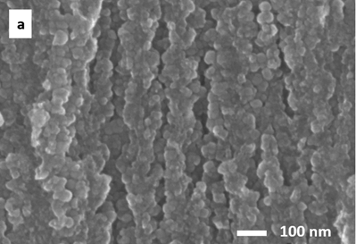
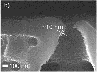
Cross-sectional SEM views of (a) mesoporous and (b) macroporous silicon after ALD TiO2 coating. The image illustrates the challenges associated with precursor transport and conformal growth inside deep porous architectures.
More broadly, this work opens perspectives for the development of three-dimensional energy devices, including porous electrodes, high aspect ratio capacitors and photo-electro-catalytic systems. It also contributes to a better understanding of ALD growth in confined and complex porous geometries [Baishya, K. et al. (2024). ACS applied materials & interfaces, 17(1), 739-749.], where precursor transport and surface reactions strongly affect the final material properties. This was done in collaboration with Central Europe Institute of Technology (CEITEC), Brno, Czechia. More details here.
6) Flexible electrodes for Li-ion batteries
Flexible macroporous silicon negative electrodes were also performed. High cycling performances were measured when using ionic liquids as electrolyte [E. Luais et al. in Journal of Solid State Electrochemistry, Vol. 23, No 3, pp 937-941, 2019] (work performed in collaboration with PCM2E lab).
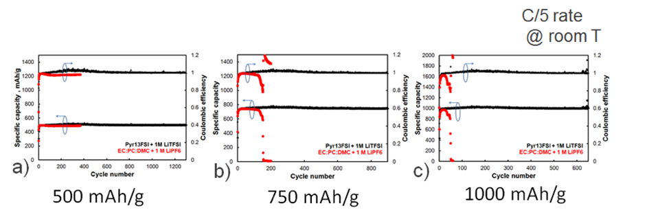
Macroporous silicon electrodes for high capacity and high cycling stability Li-ion microbatteries.
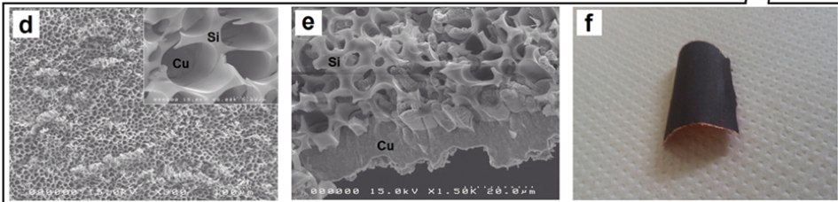
Free-standing macroporous silicon electrodes for Li-ion microbatteries as seen microscopically and macroscopically.
Porous semiconductors team
Coordinator
gael.gautier@univ-tours.fr
Permanent staff
Brice LE BORGNE
Associate researcher
Postdoc
Engineers
Anna K. OTT
Alumni
Virgil GUILLON (now: STMicroelectronics)
Lisa MONNIER (now: CHREA)