MEMS/NEMS : from design to characterization
Tools and methods
Surface micromachining processes –Top-down and bottom-up fabrication methods – Numerical and analytical models – Physical and functional characterizationCapacitive Micromachined Ultrasonic Transducers
Basic principles
Capacitive Micromachined Ultrasonic Transducers (CMUTs) are micro-membranes fabricated by means of microelectronic processes, that are actuated with electrostatic forces. The membrane (1) is made with a dielectric layer covered with a top electrode, and it moves inside a cavity in which a lower electrode is located at the bottom. The CMUT’s shape depends on the application and the vibration frequency targeted. Image (2) below shows confocal image of two square shape CMUTs.
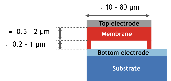
1. Cross-section view of a Capacitive Micromachined Ultrasonic Transducer.
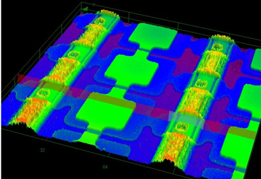
2. 2D view of two square shape capacitive micromachined ultrasonic transducers (37 x 37 µm2).
Image obtained with a confocal microscope.
Process and material characterization
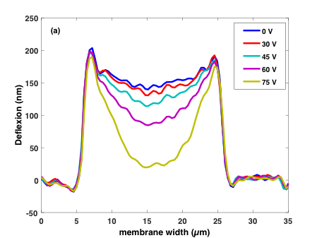
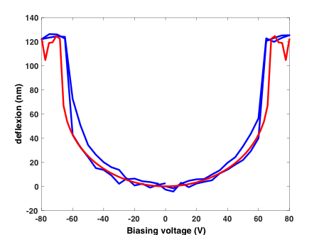
The GREMAN Laboratory developed a know-how in the design, the fabrication and the packaging (3) of CMUT technology. Our activities mainly focused on the development of process flow based on surface micromachining (4). Two processes are routinely used, a high temperature process based on LPCVD Silicon Nitride membrane and a low temperature one (< 400 °C) based on PECVD Silicon Nitride membrane (5). To help in the simulation process, characterization methods based on mechanical displacement measurements were developed1. Typically, the Displacement-Voltage curve is measured with a Digital Holography Microscope and then used, to determine2 the mechanical properties (Young’s modulus and residual stresses) of the membrane material (6).
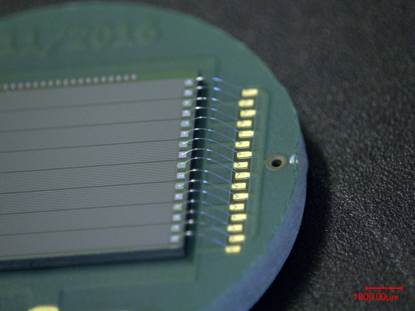

3. CMUT chip on PCB with wire-bonding electrical connections.
4. Surface micromachining process-flow.
5. 6.
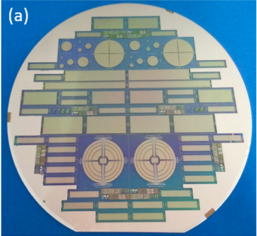
5. CMUTs realized on glass-substrate with Low Temperature surface micromachining.
6. Evolution of the static displacement of one cMUT diaphragm when a biasing voltage is applied.
(a) Displacement profile measured along the cMUT width, at the center of the diaphragm, for different biasing voltage values.
(b) Displacement measured at the center of the diaphragm (blue curve) and theory (red curve). Simulations were realized with a finite-difference model developed by our team.
Applications
A significant part of our works aims to develop the CMUT technology for ultrasonic applications, and mainly probes for ultrasound imaging, typically linear arrays development. All activities devoted to ultrasonic medical imaging applications gave rise to a specific research field that is done in the framework of the DISCUS team work.Other CMUT applications are also addressed by our group, that cover a broader field than medical arrays; from sensors, actuators to microelectronic devices:
- In a recently published paper3, it was shown that uncoated CMUT enabled to monitor gas concentration. Detection principle was based on the measurement of the CMUT membrane resonance shift caused by the gas concentration variations.
- Devices for the fabrication of mesh nebulize (7.a) were also fabricated. It consists of a Silicon membrane designed to vibrate in low frequency range, typically 100 kHz. The Silicon membrane is actuated by a CMUT array placed at the center with a dimension smaller than the membrane. A proof of concept4 was published in 2019, it was demonstrated that the second order mode was excited in water (7.b).
- Galvanic Isolation electrical transformers were fabricated. The working principle is the same than standard piezoelectric-based electrical transformers except that ultrasonic waves are emitted by CMUT array placed on each face of the transformer5. With CMUTs designed with great care, in terms of electrical resonance and anti-resonance frequencies, power transmission efficiency of 35 % were demonstrated, with a possible margin of improvement that enables to reach 60 %.

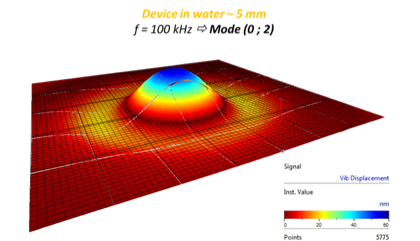
7. (a) 3D view of a CMUT-based vibrating mesh nebulizer. (b) 2D scan of the silicon membrane (in water) vibration measured at the second resonance mode (0.2).
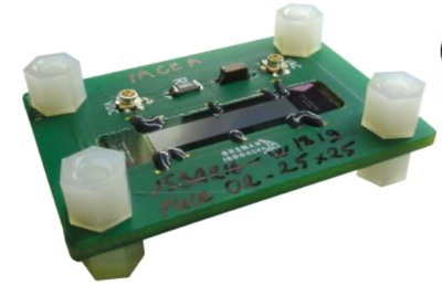
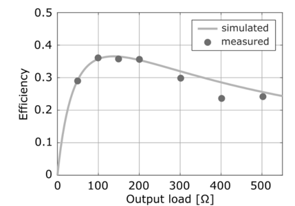
8. (a) Picture of an acoustical transformer based on CMUT technology. (b) Power efficiency measurements for different electrical output loads. The working frequency is 12 MHz.
ZnO nanowires
From the multitude of nanostructures under active research, Zinc Oxide (ZnO) nanowires (NWs) have attracted enormous attention due to the materials’ unique electrical, optical, mechanical and piezoelectric properties. During the last 10 years, piezoelectric nanocomposites based nanogenerators (NGs) have gained extensive attention for their applications in mechanical energy harvesters and self-powered tactile sensors. Among several materials, ZnO is a promising candidate: it is lead-free, has moderately high values of piezoelectric coefficients and can be grown at low temperature thanks to hydrothermal synthesis (HS).
ZnO is also a wide band gap semiconductor, with high levels of intrinsic N-type doping (in the range of 1017 or 1018 cm-3), in particular when it is produced thanks to the low temperature HS process. The free charge carriers change significantly the electric field distribution obtained by piezoelectric effect, when the device is subjected to a mechanical pressure. At GREMAN, theoretical and experimental studies are carried out to better understand the physical phenomena within the ZnO-based NGs, leading to the conversion of mechanical energy into electrical energy.
The prototype NGs are manufactured thanks to CERTeM technological platform. The well-oriented and highly crystalline ZnO NWs, shown (1), are synthesized6 by the hydrothermal reaction between 85°C and 100°C on a Au/Ti or ZnO coated substrate which may be rigid (silicon, glass) or flexible (Kapton®, PEN, PDMS). The NG manufacturing process is detailed here7 for rigid substrates, and here8 for flexible/stretchable substrates. This process is also illustrated by this video.
Different models have been developed : Mixed analytical-numerical models9, analytical models10 (2) and Finite Element models11, in order to predict the physical phenomena at the NW scale, or at the full NG device scale.
Structural12,13, electrical14,15,16 and functional17,18 characterization methods have been set up, in order to highlight the influence of HS parameters on the ZnO NWs properties19 , and the effect of the design choices on the final NG performance20,21. In particular, photoluminescence spectroscopy is performed at University of Catania22 , in order to compare the level of defects inducing excess free charge carriers, for different HS parameters or after thermal post-treatments.
In terms of performance, when the applied force on the NG device is 13 N at 5 Hz, the peak output power reaches a maximum value of 3 μW at an optimal load of 10 MΩ (4.b). Being pressed by a human palm, the peak value of open-circuit voltage and short-circuit current exceeded 27 V and 11 μA, respectively (4.c), with the peak maximum power of 35 μW at 100 kPa of compressive pressure
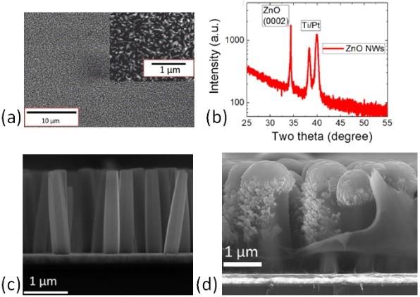
1: Top-view SEM image (a) and cross section SEM image (b) of the ZnO NWs; XRD pattern of the ZnO NWs (c), cross section SEM image (b) of the ZnO NWs covered with Parylene C and top electrode22.
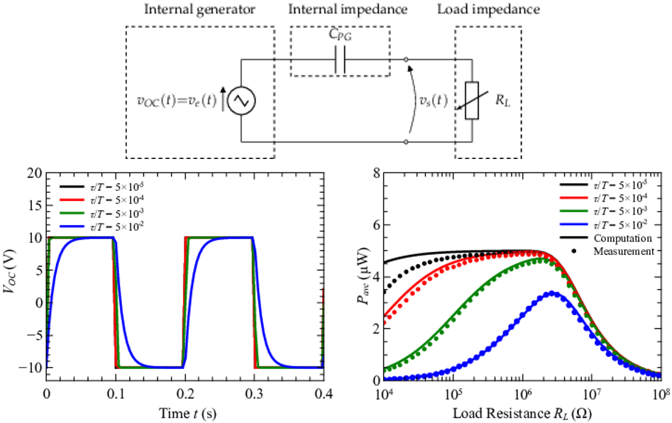
2: Equivalent circuit of the NG presenting a capacitive impedance, and connected to a resistive load; Open-circuit voltage and average power as a function of the load, for the periodic exponential signal having different values of rising time 10 .
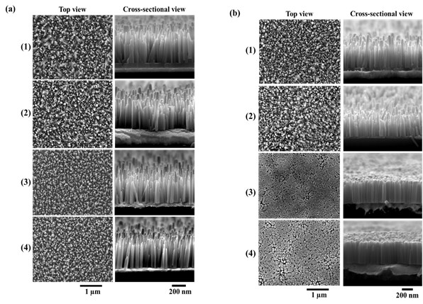
3: SEM images of ZnO NWs grown on (a) non-annealed and (b) annealed ZnO seed layers having thicknesses of (1) 100, (2) 50, (3) 10 and (4) 5 nm 21.
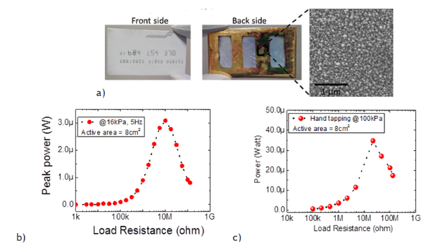
4: a) Image of the bank card and fabricated device at the back side of it. SEM image showing the as-grown ZnO NWs. Peak output power as a function of load resistance for an applied pressure of 16kPa (b) or 100 kPa (c) corresponding to hand tapping 17.
SiC cantilevers and membranes
Silicon carbide (SiC) is avowed as an interesting material for high-power and high-temperature applications because of its significant properties including its wide bandgap energy and high temperature stability. SiC is also professed as an ideal candidate to achieve MEMS, due to its excellent mechanical properties and chemical inertia, making it suitable for harsh environments.In last years, thanks to a close collaboration with CRHEA-CNRS (UPR 10), we succeeded to achieve, for the first time, a 3C-SiC micro-structure on a 3C-SiC pseudo-substrate. 3C-SiC is the cubic polytype, that can be grown on silicon substrates.
This result was attained by means of surface micromachining and using a silicon film as a sacrificial layer. Initially, the surface of the membrane was rough and faceted but thanks to an optimization of the growth, we demonstrated that smooth 3C-SiC membranes on 3C-SiC pseudo-substrates can be « easily » obtained.
laser doppler vibrometry video.
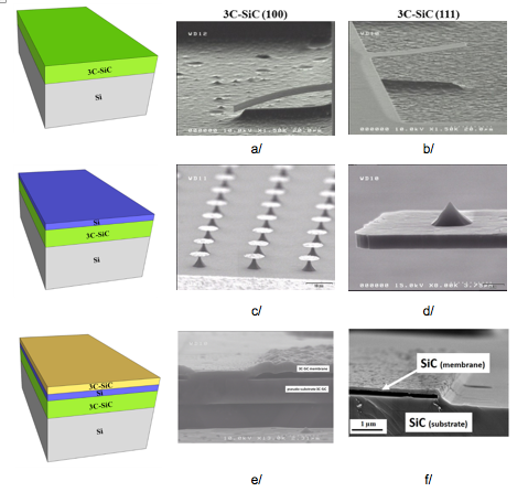
5: SEM pictures of 3C-SiC cantilevers elaborated on (a) 100-oriented material, (b) 111-oriented material, (c) monocrystalline Si tip array elaborated by ICP plasma etching and (d) the resulting final tip on a 3C-SiC cantilever, (e) first 3C‑SiC micro-structure with a 3C‑SiC membrane presenting a rough and faceted surface and (f) optimized 3C‑SiC micro-structure with a smooth 3C‑SiC membrane. For each line, the schematic illustration on the left corresponds to the heterostructure used to elaborate the devices presented on the SEM images of the right.
Considering the properties of this material, the perspectives of such a structure could be massive, for example in medical fields where the silicon carbide biocompatibility is a huge advantage. The SiC thermal properties, combined with its chemical inertia, could be also great benefits to design new MEMS devices, which could be subjected to harsh environments. The efforts developed now are then devoted to address original applications based on this structure.
Recently, we have also developed an original stitching method to characterize large 4H-SiC circular membranes. Thanks to this approach, both Young’s modulus and residual stress of 4H-SiC material were determined.
a b c d
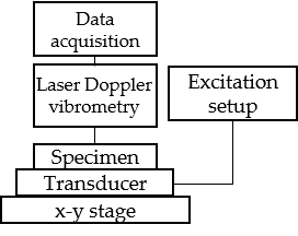
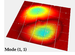
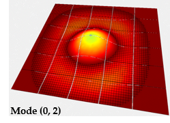
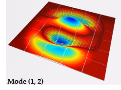
6: (a) Schematic diagram of the resonance frequency method. Vibration mode shapes measured using laser doppler vibrometry for (b) (1, 1); (c) (0, 2); and (d) (1, 2) modes (from J. Ben Messaoud et al., Micromachines 10(12), 801, 2019).
As previously explained, 3C-SiC is a very attractive material to develop sensors that can be used in harsh environments. Our group is working on this thematic in the frame of H2MEMS project. The idea is to monitor the hydrogen concentration surrounding the sensor, in a radioactive environment.
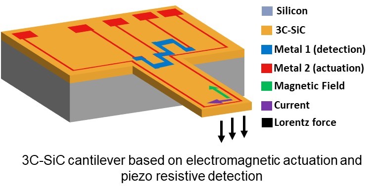
7: 3C-SiC cantilever based on electromagnetic actuation and piezoresistive detection.
