Combinatorial and Dual-PLD Thin Films synthesis
GREMAN is equipped with two Pulsed Laser Deposition systems located on two different sites which are very specific and unique in France.
Our first system is a large area and combinatorial PLD deposition tool located in the class 100 cleanroom of CERTeM PLUS technological platform on STMicroelectronics Tours site (Fig. 1).
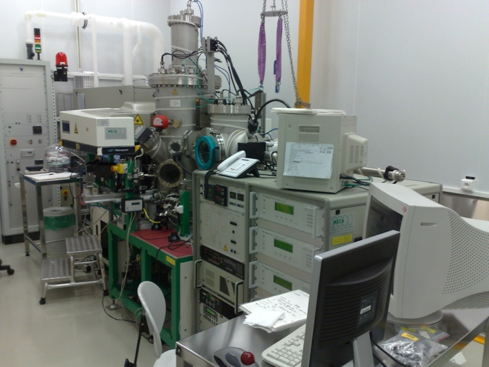
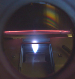
Fig.1: 6’ PLD system. On the right is a view of the 6’ heater and the plume
Characteristics of the first PLD system
- 6 inches wafer capable automatized system with wafer translations/rotation
- Homogenized and rasterized KrF excimer laser beam onto 24 selectable targets
- Temperature up to 850°C under O2/O3 ambient
- Medium pressure RHEED (up to 5 10-4 mbar)
- In-situ computer controlled shadow masking
Our second system comprising one KrF excimer laser and two PLD process chambers is located on pole EMA site. A schematic of this second system is presented in Fig. 2.
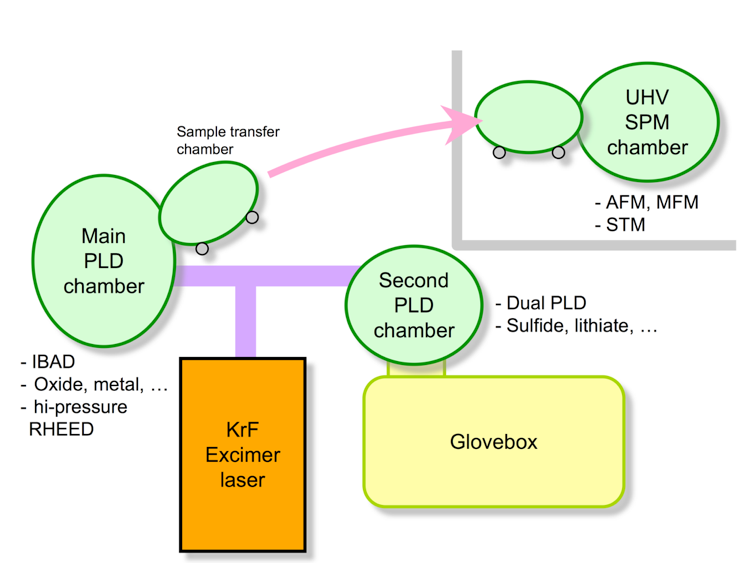
Fig. 2 : Diagram of PLD system in EMA site.
The main (#1) chamber (Fig. 3) is equipped with a high-pressure reflection high-energy electron diffraction (HP-RHEED) system, which enables us the in-situ monitoring of layer-by-layer growth of a highly- crystallized film. This chamber also possesses 2 sputter guns for metals deposition and a computer controlled mobile masque for interfaces combinatorial modulation. Attached to this chamber is a separable load lock chamber, which is also used to transfer samples from the chamber to a UHV scanning probe-microscope chamber without exposing to the air.
Fig. 3: Main (#1) and transfer chambers.
The second chamber (#2) is specialized for reactive materials including sulfides and lithiates. herefore, a glove box is combined to the chamber #2 so that one can introduce / take out the sample and target without exposing to the air (Fig. 4). The chamber #2 has a home-made two targets rotation stage for a well-controlled simultaneous ablation of two targets to achieve a dual-PLD method.
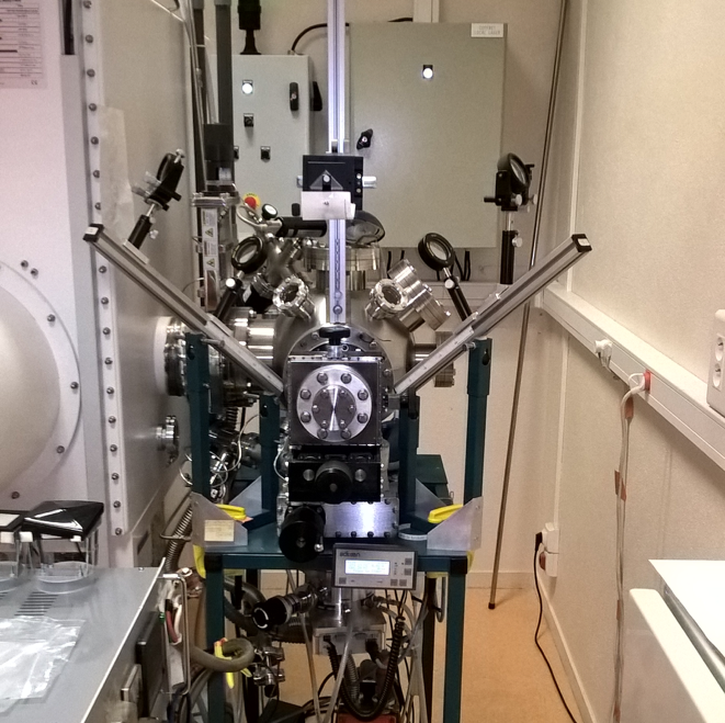
Fig. 4: Second chamber and glovebox.
Combinatorial PLD
Perovskite materials exhibit a wide range of physical properties (electrical conduction, magnetism, superconductivity, ferroelectricity, piezoelectricity…) depending on their complex composition. The stability of the perovskite structure with respect to substitution makes these materials suitable for physical properties tailoring. It is however necessary to finely screen compositions as the physical properties are extremely sensitive to composition variation.
This approach, although cumbersome for multi-cationic compound, has been widely and successfully used in bulk perovskite. The use of such materials in electronic devices requires thin film deposition with a tight control of the composition. So far most people took advantage of the good composition transfer in PLD technique for multi-cationic perovskite film growth.
Moreover, technical developments of PLD in the last decade have enabled the control of the film deposition at the atomic level through layer by layer growth (LBL). In our systems we inserted a computer controlled mask with an aperture between the substrate and the target to deposit in selected area of the substrate surface (shadow masking deposition). Synchronizing mask movements, targets selection and laser firing in a programmed sequence, it is possible to laterally modulate the composition. To ensure a good homogeneity along the growth direction, the programed sequence corresponds to the deposition of a single unit cell (u.c.) thick film with a laterally modulated composition. Mixing of the cations coming from the various targets is thus achieved at the u.c. level. Repetition of the sequence then leads to the desired film thickness. A schematic of the deposition sequence for a sample obtained with two targets is shown in Fig. 1.
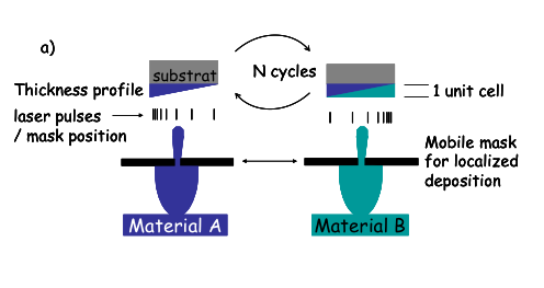
Fig. 1: Schematic of combinatorial deposition sequence
This way we synthetize material libraries with continuous composition variation on
1 cm2 substrate. Investigation of these libraries then requires local characterization tools. Examples of EDX and XRD micro-analysis of libraries are presented in Fig. 2.
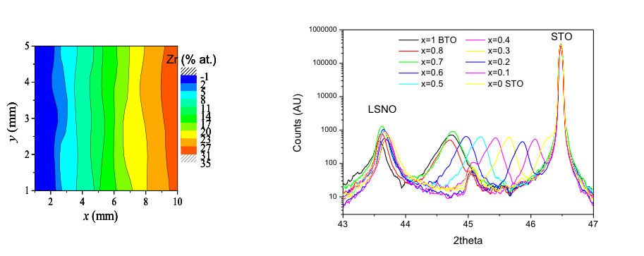
Fig. 2: Zr content in a Ba0.6Sr0.4Ti1-xZrxO3 library by EDX (left). XRD diagrams of a Ba1-xSrxTiO3 library deposited on LaSrNiO4/SrTiO3 (right)
The combinatorial deposition approach can be used for single layer phase diagram exploration as well as multilayer device optimization. Besides composition, the role played by the microstructure in the devices performances can also be investigated.
Dual PLD
A simultaneous ablation of two targets by two laser beams, namely dual-PLD, is a method that would extend the degree of freedom of material synthesis. We have established a dual-PLD scheme in which one excimer laser beam is divided into two parts by a prism. The position of this prism can be mechanically controlled so that the ablation ratio of two targets A and B is varied systematically.
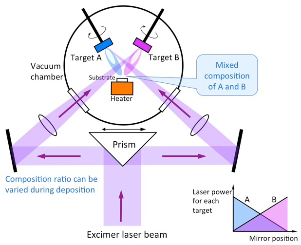
Fig. 3: Schematic of dual-PLD system

Fig. 4: Simultaneous laser ablation at two targets in the dual-PLD system.
One can switch the laser power ratio for targets (A, B) between (100, 0) and (0, 100) digitally and cyclically to prepare superlattices, or even gradually to prepare out-of-plane composition-graded films. By fixing the ratio during each deposition, of course, one obtains a series of films with uniform compositions, which can work as a combinatorial library.
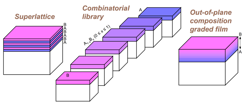
Fig. 5: Type of films that can be prepared by the dual-PLD method.
Thins films characterization and structuration:
GREMAN has access to the equipment of the CERTeM technological platform comprising:
- X-ray diffraction and micro-diffraction (-100°C; 350°C)
- SEM / FIB (FEI STRATA 400S) for TEM lamella prep
- EDX
- UV and e-beam lithography
- Ion beam milling
- Magnetron sputtering, Ion Beam Deposition, Evaporator
- Automatized electrical prober (0°C-200°C)
- Manual electrical prober (77K – 350°C)
- Ferroelectric tester (Radiant LC)
- Impedance spectroscopy (HP4294A)
- Scanning probe microscopy in air (Bruker D3100, NT-MDT LS-Solver) or vacuum (Omicron)
- Magneto-optical Kerr magnetometer and microscope
- PPMS (Quantum Design) with VSM (4K -1000K)
- Wirebonder
Deposited materials
Our field of interest covers the investigation of materials properties, in particular those related to the reduced dimension of the films, and the development of devices based on the investigated materials. The synthetized material exhibit physical properties ranging from superconductivity, ferromagnetism, high and / or tunable permittivity to piezoelectricity, insulator-metal transition. Some of the targeted applications are tunable capacitors (HF filtering), electrical control of magnetism, resistive RAM, energy harvesting and storing (Li micro-batteries). Among the pulse laser deposited films are the following materials :
Perovskite-type oxides
-
RBa2Cu3O7-x (R = Y, Nd, Pr)
-
A1-xBxMnO3 (A = La, Pr, Nd : B = Ca, Sr, Ba)
-
(Ba,Sr,Ca)(Zr,Ti)O3, CaCu3Ti4O12, LaAlO3
-
Bi1-xAxFeO3
-
SrRuO3
-
La2-xSrxNiO4
Binary oxides : TiO2, VO2, V2O3, ZnO, NiO, HfO2, SnO2, In2O3
Metals : Au, Pt, Ag, Ti…
Contact
Béatrice NEGULESCU:
beatrice.negulescu@univ-tours.fr
Jo SAKAI: jo.sakai@univ-tours.fr
Actual and former members
Ph-D students: Nazir Jaber, Romain Bodeux, Virginie Brizé
Postdoctoral fellows: Joe Sakai, Christophe Daumont, Erwan Luais, Guozhen Liu, Jie Qiu, Palash Roy Choudhury, Houssny Bouyanfif, Kesava Yellareddy, Jin-long Li, Frédéric Dumas-Bouchiat.
Partnerships and fundings
Current Fundings: Région Centre-Val de Loire, Investissements d’Avenir